
In modern SMT manufacturing, carrier tape is much more than a packaging medium. It serves as a critical interface between component packaging and automated assembly equipment. A well-designed carrier tape protects components during transportation, ensures stable feeding performance, reduces machine downtime, and improves overall production efficiency.
As electronic components continue to become smaller, lighter, and more complex, the importance of carrier tape design has increased significantly. Whether you are packaging ICs, LEDs, sensors, connectors, MEMS devices, or passive components, proper carrier tape design directly affects yield rates and assembly reliability.
This comprehensive Carrier Tape Design Guide explains the key principles, standards, materials, and engineering considerations involved in designing carrier tape solutions for modern electronic manufacturing.
What Is Carrier Tape Design?
Carrier tape design refers to the process of engineering pockets within a carrier tape that securely hold electronic components during storage, transportation, and automated pick-and-place operations.
The design process includes:
- Determining pocket dimensions
- Selecting suitable materials
- Defining component orientation
- Establishing tape width and pitch
- Ensuring cover tape compatibility
- Providing ESD protection when necessary
- Verifying feeder performance
The ultimate goal is to ensure that every component remains properly positioned throughout the entire supply chain while allowing SMT equipment to pick components efficiently and accurately.
If you are new to the packaging process, understanding the fundamentals of Carrier Tape is an excellent starting point before diving into design considerations.
Why Carrier Tape Design Matters
Many manufacturers underestimate the impact of carrier tape design until feeding problems begin affecting production.
A poorly designed tape can lead to:
- Component rotation
- Component flipping
- Pocket jamming
- Mis-picks
- Placement errors
- Increased machine stoppages
- Product damage
Even a small dimensional error can cause thousands of placement failures during high-volume SMT production.
By contrast, a properly designed carrier tape ensures:
- Reliable component retention
- Smooth feeding through automated equipment
- Consistent pick-up positions
- Lower rejection rates
- Higher production efficiency
The cost of improving carrier tape design is often far lower than the cost of production downtime caused by packaging issues.
Industry Standards That Influence Carrier Tape Design
Carrier tape designs are generally developed according to the EIA-481 standard, which defines tape-and-reel packaging requirements for electronic components.
Key specifications include:
- Tape width
- Pocket pitch
- Sprocket hole dimensions
- Pocket positioning
- Component orientation
- Cover tape alignment
Following EIA-481 standards ensures compatibility with SMT feeders used by major equipment manufacturers worldwide.
For automotive, aerospace, medical, and semiconductor applications, additional standards may also apply. Designing in accordance with industry standards minimizes compatibility risks and improves supply chain reliability.
Understanding the Key Dimensions in Carrier Tape Design
Every successful carrier tape project begins with accurate component measurement.
Component Length, Width, and Height
Engineers must evaluate:
- Overall component length
- Overall component width
- Maximum component height
- Tolerance ranges
- Lead or terminal locations
Accurate dimensional data forms the foundation of pocket design.
Even if a component appears simple, manufacturing tolerances can significantly influence pocket performance.
Pocket Length and Width
Pocket dimensions should be large enough to allow easy loading but small enough to prevent excessive movement.
If pockets are oversized:
- Components may rotate
- Feeding stability decreases
- Pick-and-place accuracy suffers
If pockets are undersized:
- Components may become damaged
- Loading becomes difficult
- Feeding resistance increases
The ideal design balances retention and accessibility.
Pocket Depth
Pocket depth must be carefully controlled.
Shallow pockets can expose components to movement and damage, while excessively deep pockets may prevent vacuum nozzles from accessing components efficiently.
Depth calculations often consider:
- Component thickness
- Cover tape clearance
- Nozzle reach capability
- Component fragility
Component Orientation
Component orientation is one of the most important design decisions.
Pick-and-place machines rely on consistent orientation to ensure accurate assembly.
Factors influencing orientation include:
- Polarity markings
- Pin 1 location
- Component geometry
- Feeder direction requirements
Incorrect orientation can create assembly errors even when the carrier tape dimensions are otherwise perfect.
Selecting the Right Carrier Tape Material
Material selection directly impacts performance, durability, and cost.
Different electronic components require different carrier tape materials depending on their sensitivity and application requirements.
Polystyrene (PS)
PS is one of the most commonly used carrier tape materials.
Advantages include:
- Cost effectiveness
- Easy thermoforming
- Good dimensional stability
- High production efficiency
PS carrier tapes are commonly used for:
- Resistors
- Capacitors
- Small IC packages
- General SMT components
PET (Polyethylene Terephthalate)
PET provides enhanced durability and environmental resistance.
Benefits include:
- Higher strength
- Better heat resistance
- Improved wear resistance
- Excellent dimensional consistency
PET is often selected for demanding industrial and automotive applications.
Polycarbonate (PC)
PC offers superior mechanical properties and transparency.
Advantages include:
- Excellent impact resistance
- High dimensional accuracy
- Strong retention capability
- Superior optical clarity
PC carrier tapes are often used for high-value semiconductor components.
The Importance of Anti-Static Design
Electrostatic discharge (ESD) represents one of the most serious risks to modern electronic components.
Sensitive devices such as:
- ICs
- MOSFETs
- Sensors
- Microprocessors
- MEMS devices
can be permanently damaged by static electricity.
For these applications, manufacturers frequently use Anti-Static Carrier Tape solutions that dissipate static charges and reduce ESD risks throughout transportation and assembly.
Anti-static carrier tapes typically incorporate conductive or dissipative additives into the material structure, ensuring compliance with industry ESD requirements.
Embossed Carrier Tape Design Principles
Most modern carrier tapes are produced using the embossed carrier tape process.
Unlike punched carrier tape, embossed carrier tape allows more sophisticated pocket geometries and tighter dimensional control.
Why Embossed Carrier Tape Dominates the Market
Benefits include:
- Better component retention
- More precise pocket dimensions
- Lower tooling costs for complex shapes
- Improved feeder compatibility
- Higher production flexibility
These advantages make Embossed Carrier Tape the preferred solution for the majority of SMT packaging applications.
Pocket Geometry Optimization
Modern pocket designs may incorporate:
- Rounded corners
- Chamfered edges
- Vacuum pickup windows
- Anti-rotation features
- Lead protection structures
These design features improve both transportation security and pick-and-place performance.
Common Carrier Tape Design Challenges
Even experienced manufacturers encounter design challenges.
Component Rotation
One of the most common issues is component rotation within the pocket.
Causes include:
- Excessive pocket clearance
- Improper pocket geometry
- Inadequate retention features
Solutions often involve redesigning pocket dimensions or adding orientation controls.
Feeding Failures
Feeding failures can result from:
- Incorrect tape pitch
- Poor pocket consistency
- Material deformation
- Inaccurate sprocket hole placement
Comprehensive testing is essential to identify and eliminate feeding problems before production begins.
Cover Tape Peeling Issues
Peel force must remain within acceptable limits.
Excessive peel force can damage components, while insufficient peel force may cause cover tape lifting during shipping.
Proper material selection and sealing parameters are critical.
Static Electricity Problems
ESD issues frequently occur in low-humidity environments.
Using conductive or anti-static materials significantly reduces the likelihood of electrostatic damage.
The Custom Carrier Tape Design Process
Many electronic components require specialized packaging that cannot be accommodated by standard tape designs.
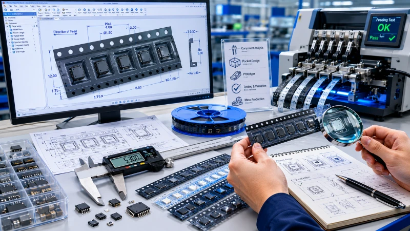
In these situations, manufacturers develop Custom Carrier Tape solutions tailored to specific component geometries.
Step 1: Component Analysis
The process begins with:
- Component samples
- Technical drawings
- 3D CAD models
- Tolerance specifications
Engineers analyze the physical characteristics of the component before developing a packaging solution.
Step 2: Pocket Engineering
Designers create pocket geometry based on:
- Retention requirements
- Feeding performance
- Component orientation
- Material properties
Advanced CAD software is typically used during this phase.
Step 3: Prototype Manufacturing
Prototype tapes are produced for validation testing.
These prototypes allow engineers to evaluate real-world performance before committing to production tooling.
Step 4: Functional Testing
Testing may include:
- Vibration testing
- Transportation simulation
- Peel force testing
- Feeder trials
- Drop testing
This stage verifies that the design performs reliably under actual operating conditions.
Step 5: Production Tooling
After validation is completed, production tooling is manufactured and mass production begins.
The result is a carrier tape solution optimized for both component protection and automated assembly.
Best Practices for Carrier Tape Design
Successful carrier tape projects often follow several key principles.
Minimize Component Movement
Allow sufficient clearance without creating excessive free space.
Consider SMT Equipment Early
Design decisions should account for feeder and pick-and-place requirements from the beginning.
Prioritize ESD Protection
When packaging sensitive devices, anti-static materials should be considered a requirement rather than an option.
Validate Through Testing
Simulation alone is not enough.
Physical testing remains essential for verifying performance.
Partner With Experienced Suppliers
Experienced carrier tape manufacturers can identify potential issues before tooling investment occurs, reducing development costs and accelerating project timelines.
Future Trends in Carrier Tape Design
As the electronics industry evolves, carrier tape technology continues to advance.
Several trends are shaping the future of carrier tape design:
- Ultra-miniature component packaging
- Higher SMT production speeds
- Improved ESD protection technologies
- Sustainable recyclable materials
- AI-assisted packaging optimization
- Smart manufacturing integration
These developments will require increasingly sophisticated carrier tape solutions capable of meeting the demands of next-generation electronics manufacturing.
Conclusion
Carrier tape design is a crucial engineering process that directly influences SMT production efficiency, component protection, and assembly reliability.
A successful design requires careful consideration of component dimensions, pocket geometry, material selection, ESD protection, feeder compatibility, and industry standards.
Whether you are packaging standard passive components or highly specialized semiconductor devices, investing in optimized carrier tape design can significantly improve manufacturing performance while reducing operational risks.
As electronic products continue to become smaller and more complex, the importance of intelligent carrier tape design will only continue to grow.