As electronic components become smaller and SMT production speeds continue increasing, packaging precision has become more important than ever. One of the most widely used solutions in semiconductor and electronics packaging is PS Carrier Tape.
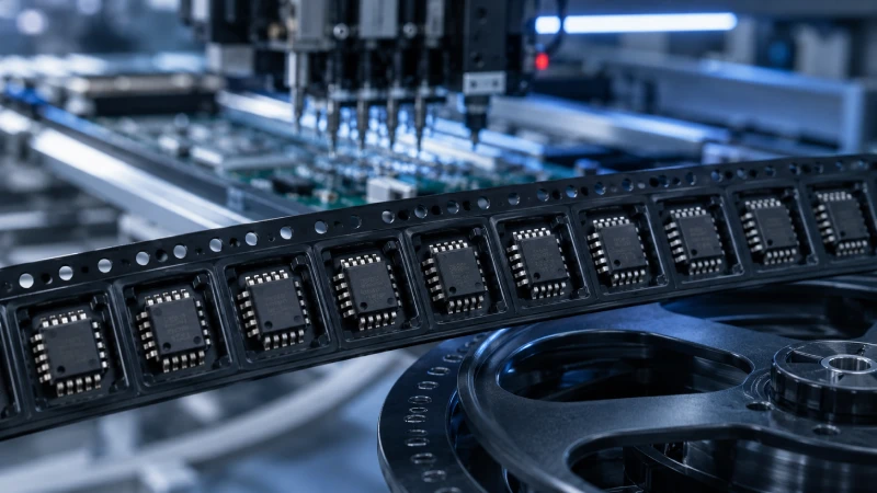
PS carrier tape, also known as polystyrene carrier tape, plays a critical role in protecting delicate electronic components during transportation, storage, and automated pick-and-place assembly. From IC chips and LEDs to connectors and precision sensors, PS embossed carrier tape helps manufacturers achieve stable feeding performance and reliable high-speed production.
Compared with other carrier tape materials, PS offers an excellent balance between rigidity, forming stability, and cost efficiency. This is why many semiconductor packaging suppliers and SMT factories still rely heavily on PS-based embossed carrier tape systems.
In this guide, you’ll learn how PS carrier tape works, its advantages, manufacturing process, common applications, and how to choose the right solution for your packaging project.
What Is PS Carrier Tape?
PS Carrier Tape is a thermoformed embossed tape made from polystyrene material. It is designed to hold and protect electronic components inside precisely formed pockets during automated tape-and-reel packaging processes.
The tape is commonly used with cover tape sealing systems and plastic reels to create standardized SMT packaging suitable for automated pick-and-place machines.
Typical PS carrier tape structures include:
- Embossed component pockets
- Sprocket holes for feeding accuracy
- Anti-static or conductive surface treatment
- Heat-sealed or pressure-sealed cover tape compatibility
PS carrier tape is widely used in industries such as:
- Semiconductor packaging
- PCB assembly
- Consumer electronics
- Automotive electronics
- LED manufacturing
- Precision sensor production
For high-speed automated production, manufacturers often integrate PS carrier tape with carrier tape packaging machines to improve efficiency and reduce manual handling errors.
Why PS Material Is Widely Used in Carrier Tape Manufacturing
Polystyrene remains one of the most popular carrier tape materials because it offers stable forming performance while maintaining relatively low production costs.
Excellent Forming Stability
PS material performs extremely well during thermoforming and embossing processes. It allows manufacturers to create highly consistent pockets with stable dimensions and smooth cavity surfaces.
This consistency is essential for high-speed SMT lines where even small dimensional deviations can cause feeding issues.
Good Rigidity for Component Protection
Compared with softer materials, PS provides strong pocket rigidity. This helps prevent component movement during transportation and reel winding.
For lightweight electronic parts such as IC chips, capacitors, and resistors, PS offers reliable protection without adding excessive packaging weight.
Cost-Effective for Large-Volume Production
Another major advantage of PS carrier tape is cost efficiency. Since many electronic packaging projects involve extremely high volumes, manufacturers need materials that balance performance with affordability.
PS helps reduce overall packaging costs while still supporting automated production requirements.
Comparison with Other Materials
| Material | Main Advantage | Common Application |
|---|---|---|
| PS | Cost-effective & rigid | General SMT packaging |
| PET | Better flexibility | Sensitive components |
| PC | Higher heat resistance | Specialized electronics |
| Paper | Eco-friendly | Lightweight components |
Although PET and PC tapes have advantages in certain applications, PS carrier tape remains the preferred solution for many standard SMT packaging environments.
Main Types of PS Carrier Tape
Different electronic components require different levels of protection and feeding performance. As a result, PS carrier tape is available in several variations.
Conductive PS Carrier Tape
Conductive PS carrier tape is designed for semiconductor and IC packaging applications that require strong ESD protection.
The conductive layer helps dissipate static electricity and reduces the risk of electrostatic discharge damaging sensitive electronic parts.
Anti-Static PS Carrier Tape
Anti-static PS tape provides moderate ESD protection for less sensitive components. It helps minimize static buildup during storage and transportation.
This type is commonly used for:
- LEDs
- Connectors
- Small electronic components
- Passive SMT devices
Clear PS Carrier Tape
Transparent or semi-transparent PS carrier tape allows easier visual inspection during packaging and quality control processes.
It is often used when operators need to inspect component orientation quickly.
Custom Embossed PS Carrier Tape
Many manufacturers require customized pocket designs based on their component dimensions.
Custom embossed carrier tape solutions may include:
- Custom pocket depth
- Special cavity geometry
- Multiple pocket configurations
- Custom reel sizes
- Specialized sprocket positioning
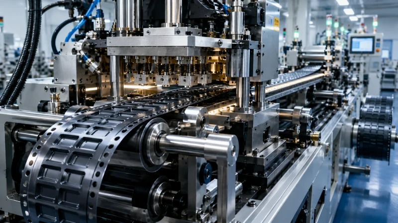
How PS Carrier Tape Is Manufactured
The manufacturing process directly affects the performance and reliability of the final carrier tape product.
Step 1 — Material Preparation
The process begins with PS resin preparation. Depending on application requirements, manufacturers may add:
- Conductive additives
- Anti-static agents
- Color masterbatch
- Performance modifiers
The material must maintain stable forming characteristics during heating.
Step 2 — Thermoforming and Embossing
The PS film is heated and passed through precision forming molds to create component pockets.
This stage determines:
- Pocket dimensional accuracy
- Surface smoothness
- Structural consistency
Even minor forming variations can impact SMT feeding performance later.
Step 3 — Sprocket Hole Punching
Accurate sprocket hole positioning is critical because automated SMT machines rely on these holes for tape feeding synchronization.
High-precision punching systems help ensure stable indexing during high-speed assembly.
Step 4 — Quality Inspection
Manufacturers perform multiple inspections during production, including:
- Pocket dimension measurement
- Material thickness verification
- Peel strength testing
- ESD performance testing
- Feeding simulation
Many suppliers use specialized carrier tape peel strength testers to ensure sealing stability between carrier tape and cover tape.
Step 5 — Reel Packaging
Finally, the finished carrier tape is wound onto reels and prepared for shipment or automated component packaging.
Fully automated systems can significantly improve consistency and reduce labor costs in large-scale production environments.
How to Choose the Right PS Carrier Tape
Selecting the wrong carrier tape can create serious production problems, including feeding failures, component loss, and SMT downtime.
Here are the key factors buyers should evaluate.
Match the Pocket Design to the Component
The pocket dimensions must fit the component precisely.
Critical considerations include:
- Width
- Depth
- Pocket pitch
- Corner geometry
- Component orientation
Oversized pockets may allow movement, while undersized pockets can damage sensitive parts.
Consider ESD Protection Requirements
Not all components require the same level of electrostatic protection.
For semiconductor devices and IC chips, conductive PS carrier tape is often recommended. For less sensitive components, anti-static solutions may be sufficient.
Evaluate SMT Feeding Stability
Stable feeding performance is essential for high-speed assembly lines.
Buyers should verify:
- Sprocket hole precision
- Cover tape compatibility
- Reel winding consistency
- Pocket dimensional tolerance
Testing samples on actual SMT equipment before mass production is highly recommended.
Work with an Experienced Carrier Tape Supplier
An experienced supplier can help optimize:
- Pocket design
- Material selection
- Reel specifications
- Packaging efficiency
This becomes especially important for irregularly shaped or miniaturized electronic components.
Common Problems with PS Carrier Tape
Even high-quality materials can encounter issues if the design or production process is not properly controlled.
Pocket Deformation
Poor forming temperatures or low-quality material can cause pocket deformation.
This may result in:
- Component instability
- Feeding errors
- Seal inconsistencies
Component Jumping
Improper pocket sizing can allow components to move inside the cavity during transportation.
This issue becomes more severe during long-distance shipping or high-speed reel handling.
Feeding Problems During SMT Assembly
If sprocket holes are not precisely aligned, SMT equipment may experience indexing problems.
This can reduce production efficiency and increase machine downtime.
ESD Failure Risks
Inconsistent conductive performance may expose sensitive electronic components to static damage.
Reliable ESD testing is therefore essential for semiconductor packaging projects.
PS Carrier Tape vs PET Carrier Tape
Many buyers compare PS and PET carrier tape before making purchasing decisions.
PS Carrier Tape Advantages
- Better rigidity
- More cost-effective
- Excellent embossing precision
- Suitable for most standard SMT packaging
PET Carrier Tape Advantages
- Better flexibility
- Improved crack resistance
- Higher transparency
- Better environmental durability
In general:
- PS is ideal for standard electronic packaging
- PET is better for specialized or high-flexibility applications
The final choice depends on component type, transportation conditions, and SMT process requirements.
Common Applications of PS Carrier Tape
PS carrier tape is widely used for packaging:
- IC chips
- LEDs
- Resistors
- Capacitors
- Connectors
- Sensors
- MOSFETs
- Precision microelectronic devices
As component sizes continue shrinking, manufacturers increasingly require high-precision embossed carrier tape systems capable of maintaining stable feeding performance under high-speed production conditions.
This demand is also driving investment in advanced automatic tape and reel packaging machines and intelligent inspection systems.
Future Trends in PS Carrier Tape Packaging
The electronics industry is rapidly evolving, and carrier tape technology is evolving with it.
Several trends are shaping the future of PS carrier tape manufacturing:
- Higher precision pocket forming
- Ultra-miniature component packaging
- Improved ESD stability
- Automated vision inspection integration
- High-speed reel packaging automation
- Environmentally optimized material development
As semiconductor packaging standards become stricter, precision manufacturing and quality control will become even more important.
Suppliers capable of offering customized embossed carrier tape solutions alongside advanced automation equipment will likely gain significant competitive advantages.
Conclusion
PS Carrier Tape remains one of the most important packaging materials in the SMT and semiconductor industries. Its combination of rigidity, dimensional stability, cost efficiency, and reliable feeding performance makes it ideal for a wide range of electronic component packaging applications.
However, achieving stable SMT production requires more than simply choosing the right material. Pocket design accuracy, ESD protection, cover tape compatibility, and manufacturing precision all play critical roles in overall packaging performance.
Whether you are packaging IC chips, LEDs, connectors, or precision electronic components, working with an experienced carrier tape manufacturer can help reduce production risks and improve assembly efficiency.