Electronic components have become smaller, more sensitive, and more complex than ever before. As a result, packaging technology plays a critical role in protecting components during transportation, storage, and automated assembly. Among the various packaging solutions used in the SMT industry, Embossed Carrier Tape has become the preferred choice for packaging integrated circuits, LEDs, connectors, sensors, and many other electronic components.
But what exactly is embossed carrier tape, how is it manufactured, and why is it so widely used in modern electronics production?
In this guide, we’ll explain everything you need to know about embossed carrier tape, including its structure, materials, advantages, applications, and how to choose the right solution for your products.
What Is Embossed Carrier Tape?
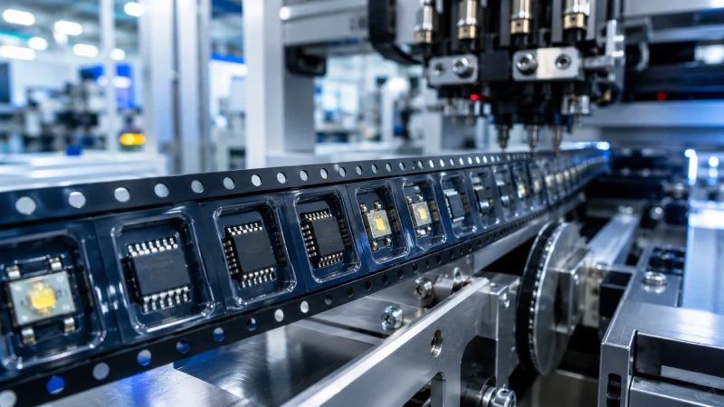
Embossed carrier tape is a thermoformed plastic tape designed with customized pockets that securely hold electronic components during handling, transportation, and automated assembly.
Unlike paper carrier tape, which uses punched cavities, embossed carrier tape is manufactured by heating and forming plastic film into precise pocket shapes. These pockets are engineered to match the dimensions of specific electronic components, ensuring reliable positioning and protection.
When combined with cover tape and reels, embossed carrier tape becomes part of a complete tape-and-reel packaging system widely used in SMT production lines worldwide.
If you’re new to component packaging, you can first learn the fundamentals of Carrier Tape before exploring embossed designs in greater detail.
Why Is Embossed Carrier Tape So Important?
Modern pick-and-place machines can place tens of thousands of components every hour. To achieve this level of efficiency, components must be delivered in a highly organized format.
Embossed carrier tape serves several important functions:
- Protects components from physical damage
- Maintains consistent component orientation
- Enables high-speed automated feeding
- Reduces handling errors
- Improves production efficiency
- Minimizes contamination risks
Without properly designed carrier tape, automated assembly would become slower, less reliable, and significantly more expensive.
How Does Embossed Carrier Tape Work?
The working principle is relatively simple but highly effective.
First, electronic components are loaded into precision-formed pockets. A cover tape is then sealed over the pockets to secure the components in place.
The tape is wound onto reels and supplied directly to SMT assembly lines.
During production:
- The feeder advances the tape.
- The cover tape peels away.
- The pick-and-place machine picks components from the pockets.
- Components are placed onto the PCB.
This process repeats continuously, allowing for extremely high assembly speeds with minimal operator intervention.
Structure of Embossed Carrier Tape
Although embossed carrier tape may appear simple, it is engineered with several critical features.
Pocket Cavity
The pocket cavity holds the component securely during transport and assembly.
Pocket dimensions are designed based on:
- Component width
- Component length
- Component height
- Component weight
- Component geometry
Sprocket Holes
Sprocket holes allow feeder systems to index the tape accurately.
Precise hole positioning is essential for smooth feeding performance.
Cover Tape Interface
The top surface is engineered to provide reliable sealing with cover tape while maintaining consistent peel strength during assembly.
Base Material
The plastic substrate determines the tape’s strength, flexibility, static performance, and dimensional stability.
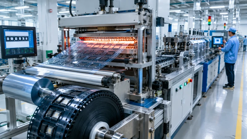
How Is Embossed Carrier Tape Manufactured?
Manufacturing embossed carrier tape requires a combination of precision tooling and quality control.
Step 1: Material Preparation
Plastic film is selected according to the application requirements.
Common materials include:
- PS (Polystyrene)
- PET (Polyethylene Terephthalate)
- PC (Polycarbonate)
- ABS
Step 2: Heating
The plastic material is heated to a controlled temperature suitable for forming.
Step 3: Thermoforming
A mold forms pockets into the heated material.
This step determines the final cavity shape and dimensions.
Step 4: Hole Punching
Sprocket holes are punched according to EIA-481 standards.
Step 5: Inspection
Quality inspections verify:
- Pocket dimensions
- Hole spacing
- Material thickness
- Surface quality
- Dimensional tolerances
Step 6: Winding
Finished tape is wound onto reels for shipment and packaging operations.
The entire process requires tight process control because even small dimensional deviations can cause feeding problems during automated assembly.
Common Materials Used for Embossed Carrier Tape
Different materials offer different performance characteristics.
Polystyrene (PS)
PS is the most commonly used material in the electronics industry.
Advantages include:
- Low cost
- Good formability
- Stable dimensions
- Suitable for most SMT applications
PET
PET provides greater strength and durability than PS.
Benefits include:
- Higher impact resistance
- Better environmental resistance
- Improved dimensional stability
PET is often used for larger or heavier components.
Polycarbonate (PC)
PC is selected when demanding performance is required.
Advantages include:
- High temperature resistance
- Excellent toughness
- Superior dimensional accuracy
ABS
ABS combines strength with flexibility.
It is commonly used for applications requiring enhanced durability during transportation and handling.
Why Anti-Static Protection Matters
Electrostatic discharge (ESD) is one of the most significant threats to electronic components.
Even a small static discharge can damage:
- Microprocessors
- ICs
- Memory chips
- Sensors
- Semiconductor devices
To prevent these issues, many manufacturers choose Anti-Static Carrier Tape for sensitive components.
Anti-static materials help:
- Dissipate static charges
- Protect sensitive electronics
- Improve product reliability
- Reduce manufacturing defects
- Meet ESD compliance requirements
As component densities continue increasing, ESD protection becomes even more critical for packaging success.
Advantages of Embossed Carrier Tape
Embossed carrier tape has become the industry standard because it offers several key advantages.
Superior Component Protection
Custom-designed pockets minimize movement during transportation.
This reduces the risk of:
- Chipping
- Scratching
- Lead deformation
- Surface contamination
High-Speed Automation Compatibility
Embossed carrier tape is specifically designed for automated assembly systems.
Reliable feeding improves:
- Placement accuracy
- Production efficiency
- Equipment utilization
Flexible Design Capability
Pocket dimensions can be customized for virtually any component shape.
This flexibility makes embossed carrier tape suitable for a wide range of industries.
Better Environmental Resistance
Plastic materials generally offer better resistance to moisture and contamination than paper alternatives.
Improved Product Presentation
Organized component packaging simplifies inventory management and production planning.
Typical Applications of Embossed Carrier Tape
Embossed carrier tape is used throughout the electronics manufacturing industry.
Integrated Circuits
IC packaging requires precise pocket dimensions to prevent damage to leads and terminals.
LEDs
LED components benefit from accurate positioning and ESD protection.
Connectors
Many connector designs feature irregular geometries that require custom pockets.
Sensors
Sensitive sensors require secure handling throughout the supply chain.
Automotive Electronics
Automotive applications demand highly reliable packaging capable of meeting strict quality requirements.
Consumer Electronics
Smartphones, tablets, wearable devices, and IoT products all rely heavily on tape-and-reel packaging.
Standard vs Custom Embossed Carrier Tape
Many manufacturers offer standard carrier tape sizes for common components.
However, standard solutions may not always provide optimal performance.
In these situations, Custom Carrier Tape becomes the preferred option.
Custom carrier tape solutions allow manufacturers to optimize:
- Pocket dimensions
- Material selection
- Static protection
- Feeding performance
- Component retention
The development process typically includes:
- Component evaluation
- Pocket design
- Tooling creation
- Sample validation
- Production approval
For unique or high-value components, custom designs often provide significant long-term benefits.
How to Choose the Right Embossed Carrier Tape
Selecting the right carrier tape requires careful evaluation of several factors.
Component Dimensions
Accurate measurements are essential for proper pocket design.
Component Shape
Complex geometries may require customized cavity designs.
Weight
Heavier components often require stronger materials.
ESD Sensitivity
Sensitive electronics should utilize anti-static materials.
Feeding Requirements
Carrier tape must be compatible with existing feeder systems.
Production Volume
Higher volumes may justify custom tooling investments.
Transportation Conditions
Environmental factors such as humidity and temperature should be considered during material selection.
Working with an experienced carrier tape manufacturer can help avoid costly packaging issues later in production.
Future Trends in Embossed Carrier Tape
As electronic devices continue shrinking, packaging requirements are becoming increasingly demanding.
Several industry trends are shaping the future of embossed carrier tape:
- Smaller and more precise pocket designs
- Enhanced ESD protection technologies
- Recyclable packaging materials
- Improved dimensional accuracy
- Automated optical inspection systems
- Smart manufacturing integration
These developments will continue improving packaging reliability while supporting increasingly advanced electronic products.
Conclusion
Embossed carrier tape is one of the most important packaging technologies in modern electronics manufacturing. By providing secure component protection, precise positioning, and compatibility with high-speed SMT assembly equipment, it enables efficient production across countless industries.
Whether you’re packaging ICs, LEDs, connectors, sensors, or automotive electronics, selecting the right embossed carrier tape can improve production efficiency, reduce defects, and enhance overall product quality.
For manufacturers requiring specialized packaging solutions, custom designs and anti-static options offer additional performance advantages that help ensure reliable results throughout the entire supply chain.