In modern electronics manufacturing, semiconductor components such as integrated circuits (ICs), sensors, and power devices require precise handling and packaging throughout production and assembly. Even minor mechanical damage, electrostatic discharge (ESD), or misalignment during automated assembly can lead to component failure, yield loss, or costly production interruptions. This is why semiconductor carrier tape plays a critical role in protecting sensitive devices and supporting reliable SMT assembly.
Semiconductor carrier tape is a key part of tape and reel packaging systems, designed to hold individual components in accurately formed pockets while enabling automated pick-and-place machines to feed them consistently during PCB assembly. By maintaining fixed spacing, protecting components from contamination or mechanical stress, and providing controlled ESD protection, carrier tape helps ensure stable handling from packaging facilities to SMT production lines.
In this guide, we explain what semiconductor carrier tape is and how engineers choose the right packaging solution for semiconductor applications.
What Is Semiconductor Carrier Tape?
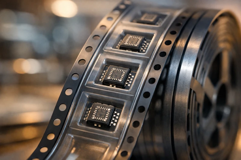
Semiconductor carrier tape is a specialized packaging material used to securely store, transport, and feed semiconductor components during automated electronics assembly. It is typically used as part of a tape and reel packaging system, where individual components are placed into precisely formed pockets along a continuous strip of carrier tape and sealed with cover tape before being wound onto a reel.
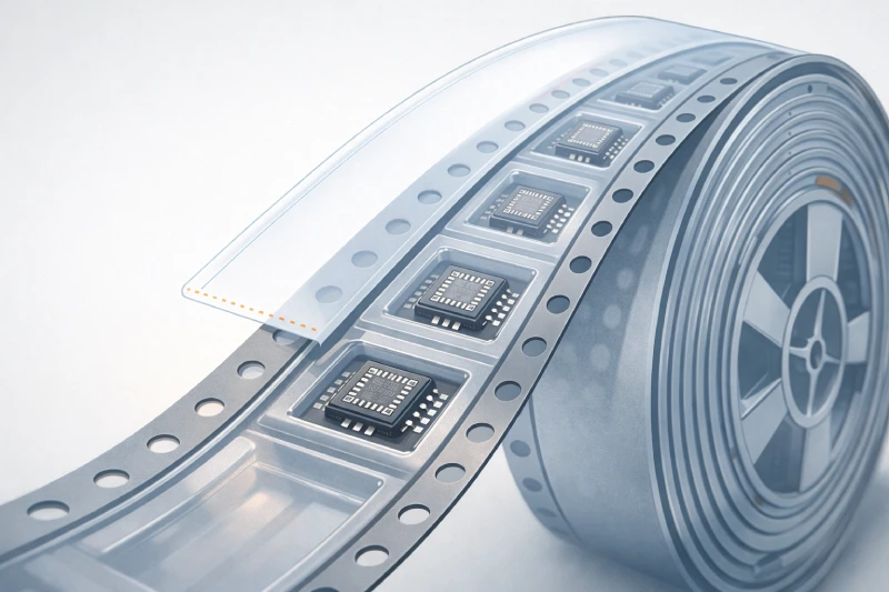
Each pocket in the carrier tape is designed to match the size and shape of the semiconductor device, ensuring the component remains stable during transportation and handling. This pocket structure prevents movement, reduces the risk of mechanical damage, and keeps components properly oriented for automated pick-and-place machines.
During SMT production, the reel is mounted onto a feeder system in the assembly line. As the tape advances, the cover tape is peeled back and the pick-and-place machine removes each component from the pocket and places it onto the printed circuit board (PCB). This controlled feeding process allows manufacturers to run high-speed, high-precision assembly operations while maintaining consistent component positioning.
For semiconductor packaging, carrier tapes are typically engineered with tight dimensional tolerances, ESD protection properties, and compatibility with industry standards such as EIA-481, ensuring reliable performance across different SMT equipment and production environments.
Why Semiconductor Components Require Specialized Carrier Tape
Semiconductor devices are significantly more sensitive than many standard electronic components, which means their packaging must provide higher levels of protection, precision, and reliability. Specialized semiconductor carrier tape is designed to meet these requirements while supporting stable handling throughout the manufacturing and assembly process.
ESD Protection
Many semiconductor devices are highly vulnerable to electrostatic discharge (ESD). Even a small static charge can damage internal circuitry or reduce long-term reliability. Semiconductor carrier tape often incorporates anti-static or conductive materials that help dissipate electrical charges and maintain a controlled electrostatic environment during storage, transportation, and assembly.
Precision Pocket Design
Semiconductor components such as IC packages, sensors, and power devices often have tight dimensional tolerances and delicate leads or contact pads. Carrier tape pockets must therefore be precisely formed to match the component geometry. Accurate pocket dimensions prevent movement inside the tape and ensure that components remain properly oriented for automated assembly.
Compatibility with High-Speed SMT Assembly
Modern SMT production lines operate at extremely high speeds. Semiconductor carrier tape must provide consistent pitch, stable pocket positioning, and reliable cover tape peeling so that pick-and-place machines can remove components smoothly without misalignment or feeding errors.
Protection During Handling and Transport
From semiconductor packaging facilities to SMT assembly plants, components may pass through multiple handling stages. Carrier tape helps protect components from mechanical shock, vibration, and contamination, ensuring they arrive at the production line in stable condition.
Common Types of Semiconductor Carrier Tape
Different semiconductor devices require different levels of protection and pocket precision. As a result, several types of carrier tape are used in semiconductor packaging, each designed to meet specific component handling and ESD protection requirements.
Embossed Carrier Tape
Embossed carrier tape is the most widely used type for semiconductor packaging. It is manufactured through a thermoforming process that creates precisely shaped pockets along the tape. These pockets are designed to match the dimensions of the semiconductor device, ensuring stable positioning during transport and automated feeding.
Because embossed carrier tape can provide high pocket accuracy and consistent spacing, it is commonly used for packaging integrated circuits (ICs), small chip packages, and various semiconductor devices used in SMT assembly.
Anti-Static Carrier Tape
Anti-static carrier tape is designed to reduce the buildup of static electricity during handling and transportation. The material surface is treated to control electrostatic charge accumulation, helping protect semiconductor components that are sensitive to ESD.
This type of tape is widely used when packaging standard ICs, sensors, and other sensitive electronic components that require a controlled electrostatic environment but do not necessarily require fully conductive materials.
Conductive Carrier Tape
Conductive carrier tape provides a higher level of electrostatic protection by allowing static charges to dissipate quickly through the tape material. It is typically used for highly sensitive semiconductor devices, including certain power devices, advanced IC packages, and components used in critical electronic systems.
By combining precise pocket forming with reliable ESD control, conductive carrier tape helps ensure safe handling throughout the semiconductor packaging and assembly process.
Carrier Tape Materials Used in Semiconductor Packaging
The performance of semiconductor carrier tape depends greatly on the material used to manufacture the tape. Different materials provide varying levels of rigidity, forming precision, and electrostatic protection. Selecting the appropriate material helps ensure that semiconductor components remain stable and protected throughout packaging, transportation, and SMT assembly.
Polystyrene (PS)
Polystyrene is one of the most commonly used materials for embossed carrier tape. It offers good formability and allows manufacturers to produce precise pocket structures with consistent dimensions. PS carrier tape is widely used for packaging many standard semiconductor devices and small IC packages.
Polycarbonate (PC)
Polycarbonate provides higher strength and durability compared with many other carrier tape materials. It maintains pocket shape stability even under demanding handling conditions, making it suitable for semiconductor components that require improved mechanical protection or tighter dimensional control.
PET (Polyethylene Terephthalate)
PET carrier tape is valued for its excellent dimensional stability and environmental resistance. It performs well under varying temperature and humidity conditions, which can be important for semiconductor logistics and long-distance transportation.
Conductive and Anti-Static Materials
For semiconductor applications where electrostatic protection is critical, carrier tapes can be manufactured with conductive or anti-static compounds. These materials help control static buildup and reduce the risk of ESD damage during handling and assembly.
Semiconductor Carrier Tape Specifications and Standards
To ensure compatibility with automated assembly equipment, semiconductor carrier tape must follow strict dimensional standards and industry specifications. These standards define the structure of the tape, pocket spacing, and reel format so that carrier tapes can be used reliably across different SMT production lines.
The most widely recognized specification is the EIA-481 standard, which defines the requirements for tape-and-reel packaging used in electronic component handling. This standard ensures that semiconductor carrier tapes are compatible with common pick-and-place machines and feeder systems used in SMT assembly.
Key specifications defined in EIA-481 include tape width, pocket pitch, pocket depth, and sprocket hole positioning. These parameters ensure that components remain properly aligned during feeding and can be consistently picked by automated equipment.
Another important factor is pocket design accuracy. The pocket must securely hold the semiconductor component while still allowing the pick-and-place nozzle to retrieve the device easily. If the pocket is too tight or too loose, it can lead to feeding problems or component misplacement.
Carrier tapes must also be compatible with the cover tape peeling process, which exposes each component as the tape advances through the feeder. Proper peeling force ensures stable operation without damaging the semiconductor devices.
How to Choose the Right Semiconductor Carrier Tape
Selecting the appropriate semiconductor carrier tape is essential for ensuring smooth SMT production and protecting sensitive components during handling and transportation. Engineers typically evaluate several key factors before choosing a carrier tape solution for semiconductor packaging.
Component Dimensions and Package Type
The first consideration is the size and shape of the semiconductor device. Carrier tape pockets must match the component dimensions closely to prevent movement inside the pocket. Accurate pocket design helps maintain proper orientation and ensures that pick-and-place machines can retrieve components reliably during high-speed assembly.
Required ESD Protection Level
Many semiconductor devices require controlled electrostatic environments. Depending on the sensitivity of the component, manufacturers may select anti-static or conductive carrier tape to prevent electrostatic discharge during storage, transport, and assembly.
Pocket Design and Forming Precision
For semiconductor components with fine leads or delicate contact pads, precise pocket forming is critical. High-quality carrier tape ensures consistent pocket dimensions, which helps reduce feeding errors and improves assembly stability on automated SMT lines.
Compatibility with Pick-and-Place Equipment
Carrier tape must meet the dimensional requirements of feeder systems and placement machines. Proper tape pitch, sprocket hole alignment, and cover tape peeling performance ensure stable and continuous feeding during automated assembly operations.
Production Volume and Packaging Efficiency
High-volume semiconductor manufacturing requires packaging solutions that support efficient automation and logistics. Selecting the correct carrier tape design improves handling reliability and overall packaging efficiency.
When Custom Semiconductor Carrier Tape Is Required
While many semiconductor components can be packaged using standard carrier tape sizes, some applications require custom carrier tape designs to ensure proper protection and feeding performance. Custom solutions are typically needed when component geometry or packaging requirements fall outside standard specifications.
One common situation is when semiconductor devices have non-standard package dimensions or unique shapes. In these cases, standard pocket designs may not provide adequate stability. Custom pocket forming allows manufacturers to create tape pockets that precisely match the component structure, ensuring reliable positioning during transportation and automated assembly.
Custom carrier tape is also often required for advanced semiconductor packages, such as MEMS sensors, specialized IC packages, and wafer-level components. These devices may require tighter pocket tolerances or specific pocket depths to prevent movement and protect sensitive contact surfaces.
In addition, industries such as automotive electronics and industrial control systems frequently require customized packaging solutions to meet strict reliability standards. Custom carrier tape helps ensure consistent component handling while supporting high-speed SMT production.
By designing pockets specifically for the semiconductor device, custom carrier tape improves packaging stability, assembly efficiency, and overall production reliability.
FAQ
What standard defines semiconductor carrier tape dimensions?
The most widely used specification for carrier tape packaging is EIA-481, an industry standard that defines tape width, pocket pitch, sprocket hole placement, and reel format. By following this standard, semiconductor carrier tapes remain compatible with a wide range of SMT feeders and automated pick-and-place equipment used in electronics manufacturing.
What is the difference between embossed carrier tape and punched carrier tape?
Embossed carrier tape is formed using thermoforming processes that create pockets designed specifically for the component shape. This makes it suitable for most semiconductor devices. Punched carrier tape, on the other hand, is produced by mechanically punching cavities into the tape and is typically used for simpler electronic components rather than precision semiconductor packages.
Does semiconductor carrier tape need ESD protection?
In most cases, semiconductor packaging requires ESD-safe materials. Anti-static or conductive carrier tape helps prevent electrostatic charge buildup during storage, transportation, and automated assembly, reducing the risk of damage to sensitive semiconductor devices.
Can semiconductor carrier tape be customized?
Yes. When semiconductor components have non-standard dimensions or specialized packaging requirements, manufacturers can design custom carrier tape pockets to match the device geometry and ensure reliable feeding during SMT assembly.
Choosing a Reliable Semiconductor Carrier Tape Manufacturer
Selecting a reliable semiconductor carrier tape manufacturer is essential for maintaining consistent packaging quality and stable SMT production. A qualified supplier should have strong engineering capabilities and experience in semiconductor packaging, ensuring that carrier tape designs meet the dimensional accuracy required for automated assembly.
Manufacturers should also comply with industry standards such as EIA-481, ensuring compatibility with common SMT feeder systems and pick-and-place equipment. Consistent pocket forming precision, stable tape materials, and reliable cover tape performance are key factors that help prevent feeding issues during high-speed production.
In addition, experienced manufacturers can provide custom carrier tape solutions when standard specifications do not meet the requirements of specialized semiconductor packages. This includes pocket design optimization, material selection, and tooling development.
Working with a trusted carrier tape manufacturer helps ensure stable component protection, reliable assembly performance, and efficient semiconductor packaging operations.