In SMT and semiconductor packaging, engineers often encounter two common carrier tape terms: Embossed Carrier Tape and Anti-Static Carrier Tape. While both are widely used in tape-and-reel packaging, they are frequently misunderstood as interchangeable options.
In reality, these two concepts address different engineering requirements. Embossed carrier tape refers to a structural forming method used to create pockets that hold components securely, ensuring consistent positioning and feeding during automated SMT assembly. Anti-static carrier tape, on the other hand, refers to material properties designed to reduce electrostatic charge accumulation and prevent ESD damage.
Because these two characteristics operate on different levels—mechanical structure vs. material conductivity—many carrier tape solutions in real production environments combine both features. Understanding the difference is critical for packaging engineers and procurement teams evaluating carrier tape solutions for specific components, SMT speeds, and ESD sensitivity levels.
This guide explains how embossed and anti-static carrier tapes differ, when each becomes necessary, and how engineers determine the appropriate option for their packaging process.
What Problem Does Each Carrier Tape Type Actually Solve?
To understand the difference between embossed and anti-static carrier tape, it is important to recognize that each solves a different problem within the SMT packaging process.
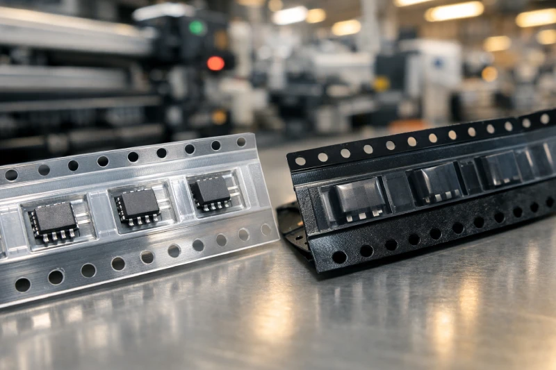
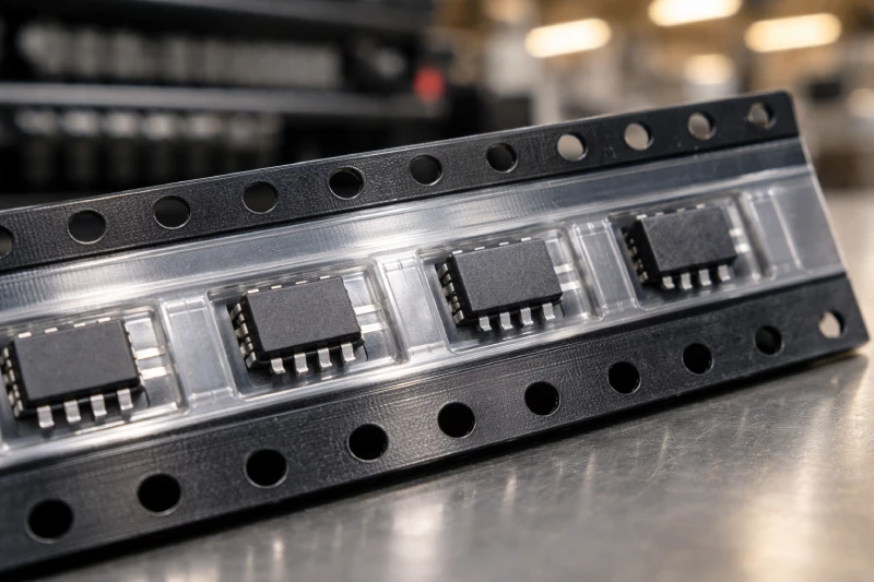
Embossed carrier tape focuses on mechanical containment and feeding stability. The embossed forming process creates precisely shaped pockets that hold electronic components in fixed positions during transportation and automated assembly. These pockets prevent components from shifting, flipping, or misaligning while the tape advances through SMT feeders.
This structural design becomes particularly important in high-speed assembly lines where consistent feeding is essential. Without properly formed pockets, components can tilt or overlap, increasing the risk of pick-and-place errors.
Anti-static carrier tape, by contrast, addresses electrostatic discharge (ESD) protection. Electronic components—especially semiconductor devices—can be damaged by electrostatic charges accumulated during handling, packaging, or transportation.
Anti-static materials reduce charge buildup by allowing controlled dissipation of static electricity. This helps prevent sudden electrostatic discharge events that could degrade sensitive components.
In short:
- Embossed carrier tape solves mechanical packaging and feeding issues
- Anti-static carrier tape solves electrostatic protection issues
These functions operate independently, which is why they should not be treated as equivalent specifications.
Is Embossed Carrier Tape Always Anti-Static by Default?
One of the most common misconceptions in SMT packaging is the assumption that embossed carrier tape automatically provides anti-static protection. In practice, this is not always the case.
The term embossed simply describes the manufacturing process used to form pockets in the tape material. During production, plastic sheets are thermoformed or embossed to create cavities that match the shape and size of electronic components.
However, the embossed forming process itself does not determine the electrical properties of the material.
Electrostatic behavior depends on the material formulation used to manufacture the tape. Different carrier tape materials can exhibit different electrical characteristics depending on additives, fillers, or coatings used during production.
For example:
- Standard PS (polystyrene) carrier tape may provide minimal static control
- Anti-static PS or PET carrier tape contains additives that allow charge dissipation
- Conductive carrier tape includes carbon-based fillers that actively conduct electricity
Because of this variation, embossed carrier tapes may fall into several categories:
- Non-ESD controlled tape
- Anti-static carrier tape
- Conductive carrier tape
For ESD-sensitive components, engineers must verify the tape’s surface resistivity and ESD classification, rather than assuming the embossed structure alone provides protection.
How Do Component Types Influence the Carrier Tape Choice?
The type of electronic component being packaged plays a major role in determining whether anti-static carrier tape is required.
Some components have relatively low ESD sensitivity, meaning they are less likely to be damaged by small electrostatic discharges. Others—particularly semiconductor devices—can be extremely sensitive to even minor charge events.
For example, passive components such as resistors or ceramic capacitors generally require reliable mechanical positioning but have relatively low electrostatic sensitivity. In these cases, embossed carrier tape with standard material properties may be sufficient.
LED components, particularly small surface-mount LEDs, require well-designed pocket structures to prevent movement or orientation issues during feeding. Depending on the LED design and manufacturing process, anti-static materials may also be recommended to reduce handling risks.
For integrated circuits and semiconductor devices, electrostatic protection becomes much more critical. These components often require carrier tapes with anti-static or conductive properties to maintain safe ESD levels throughout the packaging and assembly process.
Connectors and mechanical components, on the other hand, typically prioritize pocket strength and mechanical stability rather than electrostatic protection.
As a result, the correct carrier tape choice depends on both the mechanical characteristics of the component and its ESD sensitivity level.
How Does ESD Risk Affect Tape Material Selection?
Electrostatic discharge can occur at several stages during electronic component handling, making ESD risk evaluation a key factor when selecting carrier tape materials.
Static charges may accumulate during:
- Component loading into the carrier tape
- Tape winding and reel handling
- Transportation and storage
- Automated feeding within SMT machines
If electrostatic charges accumulate on packaging materials, they can discharge suddenly when the component contacts grounded equipment or conductive surfaces.
The severity of this risk depends on several factors, including:
- The ESD sensitivity of the component
- Environmental conditions such as humidity levels
- Grounding conditions within the production line
- The level of automation and handling frequency
To mitigate these risks, carrier tape materials may be formulated to provide controlled static dissipation.
Common ESD-safe carrier tape materials include:
- Anti-static PS carrier tape for general electronics packaging
- Anti-static PET carrier tape for improved dimensional stability
- Conductive carrier tape materials for highly sensitive semiconductor components
Selecting the correct material ensures that electrostatic charges do not accumulate during packaging, storage, or automated assembly.
Can One Carrier Tape Combine Embossed Structure and Anti-Static Properties?
Yes. In modern SMT packaging systems, most carrier tape solutions combine embossed pocket structures with anti-static or conductive material properties.
This combination is necessary because electronic packaging must simultaneously satisfy mechanical stability and electrostatic safety requirements.
The embossed structure ensures that components remain securely positioned during transportation and feeding. At the same time, the anti-static or conductive material formulation helps prevent static charge accumulation on the tape surface.
Several engineering approaches are used to achieve this combination:
- Using anti-static PET or PS materials during tape extrusion
- Adding carbon-based conductive fillers to the polymer
- Applying anti-static surface coatings to the tape material
These design strategies allow the carrier tape to provide both structural accuracy and electrostatic protection without compromising pocket quality or feeding performance.
As a result, embossed carrier tape and anti-static carrier tape should be viewed as complementary design elements rather than competing product categories.
What Are the Practical Selection Criteria for SMT Packaging Engineers?
Selecting the correct carrier tape involves evaluating several practical engineering factors related to both component protection and SMT process stability.
First, engineers must consider the ESD sensitivity level of the component. Semiconductor devices typically require anti-static or conductive materials, while less sensitive components may not.
Second, the pocket geometry and component dimensions must be matched precisely to ensure reliable mechanical containment.
Third, the tape material itself plays an important role in maintaining dimensional stability, especially in high-speed production environments.
Additional considerations include:
- Compatibility with SMT feeder systems
- Consistency of pocket spacing and depth
- Resistance to deformation during reel winding
- Performance under high-speed SMT placement conditions
High-volume assembly lines operating above tens of thousands of components per hour rely heavily on consistent carrier tape performance. Even minor variations in pocket structure or material properties can lead to feeder jams or pick errors.
For this reason, many engineers evaluate carrier tape solutions based on both mechanical design precision and material characteristics.
When Should You Consider Custom Carrier Tape Solutions?
Standard carrier tape formats are suitable for many common electronic components. However, certain packaging situations require custom carrier tape solutions.
Custom designs become necessary when components have unusual shapes, fragile structures, or unique handling requirements that standard pocket geometries cannot accommodate.
Typical cases include:
- Components with irregular geometry
- Ultra-small semiconductor packages
- Delicate components prone to movement or rotation
- Packaging processes requiring strict ESD control
Custom carrier tape development allows engineers to optimize multiple design parameters simultaneously, including pocket structure, material conductivity, and dimensional tolerances.
By tailoring the tape design to specific component requirements, manufacturers can improve feeding reliability, reduce packaging damage, and maintain consistent SMT assembly performance.
Many SMT packaging projects therefore combine custom embossed pocket designs with anti-static or conductive materials to achieve the required balance of protection and process stability.
Conclusion
Embossed carrier tape and anti-static carrier tape address two different but equally important aspects of electronic component packaging.
Embossed carrier tape provides the mechanical structure required for accurate component positioning and stable SMT feeding, while anti-static carrier tape ensures electrostatic safety during handling, storage, and assembly.
In most modern SMT packaging solutions, these two characteristics are combined within the same tape design. The correct choice ultimately depends on the component’s ESD sensitivity, mechanical requirements, and the operating conditions of the SMT production line.
By understanding how these factors interact, engineers and procurement teams can select carrier tape solutions that support both component protection and reliable automated assembly.