Introduction
In semiconductor manufacturing and SMT assembly, packaging is not just about protection—it directly affects production yield, feeding stability, and component reliability. Chip carrier tape is a specialized form of carrier tape designed specifically for integrated circuits (ICs) and high-value semiconductor components, where precision and consistency are critical.
Unlike general-purpose tapes used for passive components, chip carrier tape must meet tighter dimensional tolerances, provide reliable electrostatic discharge (ESD) protection, and ensure stable feeding at high placement speeds. Even minor design mismatches can lead to issues such as chip rotation, pick-and-place errors, or electrostatic damage.
Understanding how chip carrier tape works—and how to select the right configuration—is essential for engineers, procurement teams, and packaging specialists aiming to reduce defects and improve SMT efficiency.
What Is Chip Carrier Tape and How It Works
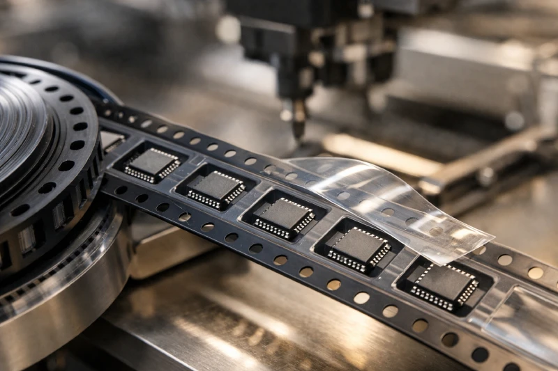
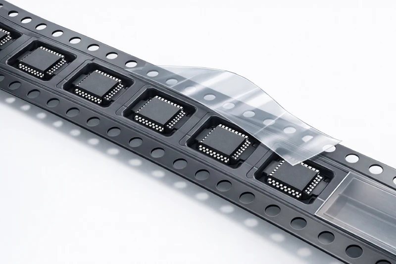
Chip carrier tape is a precision-engineered packaging medium used to store, protect, and transport semiconductor components within tape and reel systems. It is widely used in automated SMT assembly, where components are fed into pick-and-place machines at high speed.
The tape consists of several key structural elements:
- Pockets (cavities): Designed to securely hold individual chips
- Pitch: The spacing between pockets, ensuring synchronized feeding
- Sprocket holes: Used by feeders to index and advance the tape
- Cover tape: Seals components in place and protects them during transport
In a typical workflow, components are loaded into the pockets, sealed with cover tape, and wound onto reels. During SMT assembly, feeders pull the tape forward while peeling off the cover tape, allowing pick-and-place heads to retrieve each component.
Compared to standard carrier tape, chip carrier tape is engineered with tighter pocket tolerances and enhanced material properties to prevent movement, flipping, or damage—especially for delicate IC packages.
Key Design Parameters of Chip Carrier Tape
The performance of chip carrier tape is defined by its design precision. Small variations in geometry or material can significantly impact feeding stability and component integrity.
Pocket Dimensions and Tolerance
Pocket design must closely match the chip’s dimensions, including length, width, and thickness. Excess clearance can cause rotation or misalignment, while insufficient clearance may lead to sticking or difficult pick-up.
Key considerations include:
- Controlled clearance to prevent movement
- Consistent pocket depth for vacuum pick-up
- Smooth cavity surfaces to avoid mechanical stress
For complex geometries, such as QFN or BGA packages, manufacturers often rely on embossed carrier tape to achieve precise cavity shapes.
Pitch Accuracy and Feeding Stability
Pitch accuracy determines how reliably the tape advances through SMT feeders. Any deviation in pitch can result in misalignment between the pocket and the pick-up position.
In high-speed assembly environments (e.g., above 60,000 components per hour), even slight pitch errors can lead to:
- Pick failures
- Increased machine stoppages
- Reduced placement accuracy
Maintaining tight pitch tolerances ensures smooth, uninterrupted feeding.
Material Selection (PS, PET, PC)
Material choice affects mechanical strength, transparency, thermal resistance, and ESD behavior.
- Polystyrene (PS): Cost-effective, suitable for standard IC packaging
- Polyethylene Terephthalate (PET): Transparent, ideal for optical inspection systems
- Polycarbonate (PC): High-temperature resistance for demanding environments
Selecting the appropriate material depends on component sensitivity, process conditions, and inspection requirements.
ESD and Moisture Protection for Semiconductor Chips
Semiconductor devices are highly sensitive to electrostatic discharge. Even low-voltage ESD events can cause latent defects that are difficult to detect during inspection but lead to field failures.
Chip carrier tape addresses this through:
- Conductive materials: Provide controlled dissipation paths
- Anti-static coatings: Prevent charge accumulation during handling
These solutions are commonly integrated into anti-static carrier tape configurations.
Moisture Sensitivity Considerations
Many IC packages are classified under Moisture Sensitivity Levels (MSL), meaning they can absorb moisture from the environment. Improper handling may result in:
- Popcorning during reflow
- Internal structural damage
- Reduced device reliability
Carrier tape works in combination with dry packing, desiccants, and moisture barrier bags to protect sensitive components throughout storage and transportation.
Common Problems in Chip Carrier Tape Applications
Even with high-quality materials, improper design or selection can lead to recurring production issues. Understanding these problems helps identify root causes and prevent yield loss.
Chip Rotation or Misalignment
Oversized pockets or poor cavity geometry can allow chips to rotate or shift within the pocket. This leads to incorrect orientation during pick-up and placement errors.
Feeding Issues in SMT Machines
Feeding instability is often caused by:
- Inconsistent pitch spacing
- Misaligned sprocket holes
- Tape deformation
These issues disrupt synchronization between the feeder and placement head.
Cover Tape Peeling Problems
Peel force must be carefully controlled. If it is too high, components may lift or shift; if too low, sealing integrity is compromised.
Unstable peeling can result in:
- Component loss
- Flying parts during high-speed operation
- Increased downtime
Electrostatic Damage (ESD Failures)
Without proper ESD protection, chips may experience silent damage that passes initial inspection but fails later in the field.
When standard solutions cannot resolve these issues, many manufacturers turn to custom carrier tape designs to optimize pocket geometry, materials, and performance.
Standard vs Custom Chip Carrier Tape: When to Choose Each
Selecting between standard and custom carrier tape depends on component type, production volume, and quality requirements.
Standard Carrier Tape
- Lower cost and faster availability
- Suitable for widely used packages (e.g., SOP, SOT)
- Adequate for general-purpose applications
Custom Carrier Tape
- Designed for unique or high-value components
- Optimized pocket dimensions and tolerances
- Improved feeding reliability and reduced defects
Custom solutions are particularly important for advanced semiconductor packages such as QFN, BGA, or irregularly shaped ICs.
How to Select the Right Chip Carrier Tape (Step-by-Step)
Choosing the correct chip carrier tape requires a structured evaluation process.
Step 1: Define Component Dimensions
Accurately measure length, width, thickness, and allowable tolerances. This ensures proper pocket design and prevents movement.
Step 2: Determine Material Requirements
Consider:
- ESD sensitivity
- Transparency for inspection
- Thermal resistance
Step 3: Match Packaging Type
Different package types require different pocket geometries. For example:
- Flat packages need shallow pockets
- Ball grid arrays require deeper cavities
Step 4: Validate Peel Force
Ensure that cover tape peeling is stable and consistent across production conditions. This directly affects feeding performance.
Step 5: Conduct Trial Runs
Before full-scale production, test the tape in real SMT conditions. Evaluate:
- Feeding smoothness
- Pick accuracy
- Defect rates
Working with a supplier that offers integrated tape and reel packaging solutions can streamline this validation process and reduce implementation risk.
Industry Standards for Chip Carrier Tape (EIA-481 Explained)
EIA-481 is the primary industry standard governing tape and reel packaging for electronic components. It defines critical parameters such as:
- Tape width and pocket dimensions
- Sprocket hole positioning
- Reel size and configuration
Compliance with EIA-481 ensures compatibility across different SMT equipment and global supply chains. It also minimizes integration issues when sourcing components from multiple suppliers.
For manufacturers and buyers, adherence to this standard is not optional—it is essential for maintaining consistent quality and operational efficiency.
Conclusion: Why Chip Carrier Tape Quality Directly Impacts Yield
Chip carrier tape plays a far more critical role than simple packaging. It directly influences how components are handled, fed, and placed during SMT assembly.
Precision in pocket design, material selection, and ESD protection determines whether production runs smoothly or suffers from recurring defects. Poorly designed tape can lead to misalignment, feeding errors, and hidden reliability risks.
For high-value semiconductor components, investing in properly engineered carrier tape solutions is a practical way to reduce defects, improve yield, and ensure long-term product reliability.