Integrated circuits and electronic components are becoming smaller, more delicate, and more expensive. During transportation and SMT assembly, even a minor issue such as static discharge, incorrect orientation, or unstable feeding can damage parts or stop production.
That is why carrier tape plays a critical role in tape and reel packaging. A properly designed carrier tape keeps every component in the correct position, protects it during shipping, and ensures smooth feeding into automated pick-and-place machines.
For ICs, semiconductors, LEDs, connectors, and other sensitive electronic components, choosing the wrong tape can lead to misfeeds, cracked parts, static damage, and costly downtime. In contrast, the right carrier tape improves SMT efficiency, lowers defect rates, and protects product quality.
If you need a tape design for a new component, it is best to evaluate the package size, ESD requirement, pocket design, and cover tape compatibility before production begins.
What Is Carrier Tape for IC and Electronic Components?
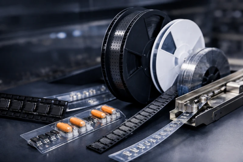
Carrier tape is a thermoformed or punched plastic tape used to hold electronic components in individual pockets. The tape is sealed with a cover tape and then wound onto a reel so the parts can be transported and automatically fed into SMT equipment.
In tape and reel packaging, the carrier tape, cover tape, and plastic reel work together as a complete system. The carrier tape creates the pocket that holds the component, the cover tape keeps the part in place, and the reel allows the tape to feed smoothly through the SMT machine.
ICs, chips, LEDs, connectors, resistors, capacitors, and sensors are all commonly packaged in carrier tape. Each part sits in its own pocket with a specific orientation so the pick-and-place machine can identify and place it correctly.
For many semiconductor devices, even a small dimensional error can cause the part to rotate, tilt, or jam during feeding. Because of this, carrier tape dimensions must match the component very closely.
For a broader overview of complete packaging systems, see the Tape & Reel Packaging Solutions page and the main Carrier Tape guide.
Which Electronic Components Commonly Use Carrier Tape?
Almost every SMT component can be supplied in carrier tape, but the tape width, pocket shape, and material vary depending on the component.
| Component Type | Typical Tape Width | Main Requirement |
|---|---|---|
| ICs and semiconductor packages | 8–24 mm | Precise orientation and ESD protection |
| Resistors and capacitors | 8 mm | Stable high-speed feeding |
| LEDs | 8–16 mm | Pocket depth and anti-static material |
| Connectors | 16–56 mm | Large custom pocket shape |
| Sensors and modules | 24–72 mm | Deep pockets and strong cover tape |
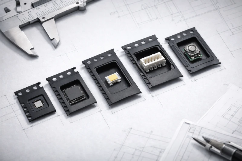
IC packages such as SOP, QFP, QFN, BGA, SOT, and DIP often require a custom pocket shape because their pins and body dimensions vary significantly. Small passive components such as resistors and capacitors usually use standard embossed carrier tape.
LEDs often require anti-static materials and carefully controlled pocket depth because they are lightweight and can easily move inside the cavity. Connectors, modules, and irregular parts typically require a fully customized pocket design.
If your component has an unusual shape or cannot feed correctly in a standard tape, a Custom Embossed Carrier Tape solution is usually required.
Types of Carrier Tape Used for IC Packaging
Several types of carrier tape are used in electronic packaging, but embossed carrier tape is the most common for ICs and SMT components.
Embossed Carrier Tape
Embossed carrier tape is made by thermoforming pockets into a plastic strip. Each pocket is designed to fit the exact dimensions of the component.
This type of tape is widely used for:
- Integrated circuits
- LEDs
- Connectors
- Sensors
- Passive SMT components
- Semiconductor packages
Embossed carrier tape provides the best pocket accuracy and feeding stability. Because the pockets can be customized, it is ideal for ICs and delicate components that require exact positioning.
Punched Carrier Tape
Punched carrier tape is made by punching holes or openings into a flat strip of material. It is usually used for simpler components or older packaging methods.
Compared with embossed tape, punched tape offers lower cost but less pocket accuracy. For modern ICs and semiconductor devices, it is rarely the best option.
Anti-Static and ESD Carrier Tape
Semiconductors and ICs are extremely sensitive to electrostatic discharge. For these applications, anti-static or ESD-safe carrier tape is essential.
An ESD carrier tape uses conductive or dissipative materials that reduce the buildup of static electricity. This protects sensitive components during packaging, transportation, storage, and SMT feeding.
For most semiconductor applications, Embossed Carrier Tape combined with Anti-Static Carrier Tape provides the safest and most reliable solution.
Why ESD Protection Matters for IC Carrier Tape
Integrated circuits may appear undamaged after a static event, but electrostatic discharge can create hidden failures that appear later in the field. These latent defects are one of the biggest risks in semiconductor packaging.
A standard plastic carrier tape may generate static electricity through friction during winding, shipping, or high-speed SMT feeding. If the component is sensitive, this static can damage the chip internally.
Common problems caused by poor ESD protection include:
- Reduced semiconductor reliability
- Intermittent product failure
- SMT assembly defects
- Lower production yield
- Customer returns and warranty claims
Different ESD materials provide different levels of protection.
| Material Type | Surface Resistance Range | Typical Application |
|---|---|---|
| Conductive | 10³–10⁵ Ω | Highly sensitive semiconductor devices |
| Dissipative | 10⁶–10⁹ Ω | Most IC and SMT applications |
| Anti-static | 10⁹–10¹² Ω | General electronic components |
Conductive materials provide the strongest protection but are not always necessary. Dissipative carrier tape is often the preferred option for most ICs because it balances protection and usability.
For chips, ICs, and semiconductor devices, an ESD-safe embossed carrier tape is usually the safest choice.
How to Choose the Right Carrier Tape for Your Component
Selecting the correct carrier tape requires more than simply choosing the right tape width. The pocket shape, material, cover tape, and SMT machine must all work together.
1. Measure the Component Dimensions
Start with the component length, width, and height. The pocket should be slightly larger than the component so it can enter the cavity easily, but not so large that the part rotates or shifts.
As a general rule, too much clearance causes unstable feeding, while too little clearance can damage the part during loading.
2. Define the Correct Orientation
ICs often require a fixed orientation so the pick-and-place machine can identify pin 1 or the correct lead direction. The pocket design must prevent the part from rotating inside the tape.
For connectors and irregular components, this is especially important.
3. Design the Pocket Carefully
Pocket design includes:
- Pocket width
- Pocket depth
- Corner radius
- Bottom support area
- Lead protection area
A poor pocket design can cause components to tilt, overlap, or become stuck. For fragile ICs, the pocket should support the body without putting pressure on the leads.
4. Choose the Right Material
The most common carrier tape materials are:
- Polystyrene (PS)
- Polycarbonate (PC)
- PET
- Conductive or dissipative versions of these materials
PS is economical and widely used for standard SMT parts. PC offers better dimensional stability and is often preferred for precision semiconductor packaging. PET provides good strength and transparency.
For components that require higher heat resistance or more durable handling, a High-Temperature Resistant Carrier Tape or High-Strength Carrier Tape may be necessary.
5. Match the Correct Cover Tape
The carrier tape must work with the correct cover tape. If the peel force is too low, components may escape from the pockets. If it is too high, the SMT machine may stop or damage the tape.
The two main options are:
- Pressure-sensitive cover tape
- Heat-activated cover tape
Pressure-sensitive tape is easier to use and suitable for many standard applications. Heat-activated tape often provides stronger sealing and is commonly used for ICs and higher-value components.
To compare these options in detail, see the guide on Heat Activated vs Pressure Sensitive Cover Tape.
Before finalizing the design, prepare the following information:
- Component drawing or sample
- Package dimensions
- Required tape width
- Reel size
- ESD requirement
- SMT machine model
Providing this information allows a carrier tape manufacturer to recommend the correct design much more quickly.
Common Carrier Tape Materials for IC and Electronic Components
Material selection directly affects forming quality, feeding reliability, and ESD performance.
| Material | Main Feature | Typical Application |
|---|---|---|
| PS (Polystyrene) | Low cost and easy to form | Standard ICs and passive parts |
| PC (Polycarbonate) | Strong and dimensionally stable | Precision IC and semiconductor packaging |
| PET | Good strength and transparency | LEDs and electronic components |
| Conductive PS or PC | ESD-safe | Sensitive ICs and chips |
PS is the most common choice because it is economical and suitable for most SMT components. However, for larger ICs or high-precision semiconductor devices, PC is often a better option because it resists deformation and maintains pocket accuracy.
PET is often used when additional strength or transparency is needed. Conductive PS and conductive PC are used when ESD protection is critical.
The correct material depends on:
- Component fragility
- Package size
- SMT speed
- Storage conditions
- ESD sensitivity
Using the wrong material can cause pocket deformation, unstable feeding, or inadequate protection.
Common Problems Caused by Poor Carrier Tape Design
A carrier tape may appear acceptable during initial testing, but problems often appear once the line begins running at high speed.
Common issues include:
- Components rotating inside the pocket
- ICs sticking to the tape because of static electricity
- Cover tape peeling incorrectly
- Pick-and-place misfeeds
- Damaged leads or cracked packages
- Production line stoppages
- Higher scrap rates and lower yield
For example, if the pocket is too shallow, the component may rise above the cavity and contact the cover tape. If the pocket is too deep, the nozzle may not pick the part correctly.
Likewise, if the tape material is not ESD-safe, lightweight ICs or LEDs may stick to the cavity because of static.
These problems can become extremely expensive once production begins. That is why many manufacturers test the tape design with sample parts before mass production.
Testing early usually costs far less than solving feeding problems later.
Custom Carrier Tape vs Standard Carrier Tape
Standard carrier tape works well for common SMT components such as resistors, capacitors, and small IC packages that follow industry-standard dimensions.
However, many electronic components do not fit into standard tape designs.
| Feature | Standard Carrier Tape | Custom Carrier Tape |
|---|---|---|
| Component Size | Standard SMT parts | Unique or irregular parts |
| Cost | Lower | Higher tooling cost |
| Lead Time | Faster | Longer development time |
| Feeding Reliability | Good for common parts | Best for difficult components |
| Best For | Resistors and capacitors | ICs, connectors, sensors, modules |
Custom carrier tape is often necessary for:
- Large connectors
- Unusual IC packages
- Sensors
- Modules
- Delicate semiconductor devices
Although a custom tool requires additional time and cost, it often improves feeding reliability and reduces defects. In many cases, the tooling cost is quickly offset by lower scrap rates and smoother SMT production.
If your part has a non-standard shape, fragile leads, or strict orientation requirements, a Custom Carrier Tape design is usually the better long-term solution.
FAQs About IC Carrier Tape
What type of carrier tape is best for ICs?
ESD-safe embossed carrier tape is usually the best choice because it combines precise pocket geometry with static protection.
Do all ICs require anti-static carrier tape?
Most ICs and semiconductor devices should use anti-static or dissipative carrier tape. Sensitive chips can be damaged by static even if no visible defect appears.
What is the standard width of carrier tape for ICs?
Most IC carrier tape widths range from 8 mm to 24 mm, although larger components may require wider tape.
Can custom-shaped components use carrier tape?
Yes. Custom embossed carrier tape can be designed for connectors, sensors, modules, and irregular electronic components.
How do I choose between heat-activated and pressure-sensitive cover tape?
The correct choice depends on the tape material, required peel force, SMT speed, and component sensitivity.
Conclusion
Carrier tape is much more than a simple packaging material. For ICs and electronic components, it directly affects product protection, SMT feeding performance, and manufacturing efficiency.
The best results usually come from combining the correct pocket design, ESD-safe material, and compatible cover tape. While standard carrier tape works for common SMT parts, sensitive ICs, connectors, and semiconductor devices often require a custom embossed design.
If you are selecting carrier tape for a new IC or electronic component, send your drawing, package dimensions, or sample for evaluation. A properly designed carrier tape can reduce defects, improve feeding reliability, and prevent costly production problems before they happen.